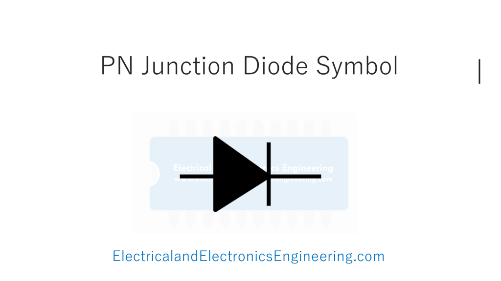
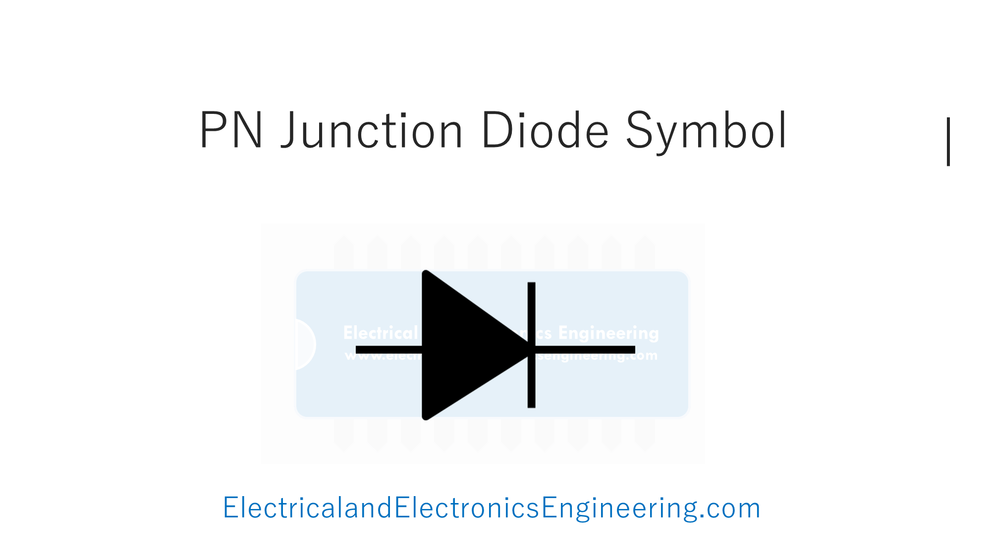
A PN junction diode is a two-terminal semiconductor device formed by the junction of P-type and N-type regions. The P-type region has an excess of positive charge carriers (holes), while the N-type region has excess negative charge carriers (electrons). The junction between the two regions forms a depletion zone where free charge carriers are depleted. When a forward bias voltage is applied across the diode, the depletion zone narrows, allowing current to flow. In reverse bias, the depletion zone widens, preventing current flow. The PN junction diode is widely used as a rectifier, voltage regulator, and signal switch in electronic circuits. The symbol for a p-n junction diode is a triangle pointing to a line. The figure below displays PN Junction Diode Symbol.
Also see complete list of Electrical and Electronics Engineering Symols here

